

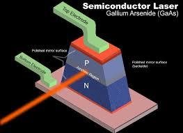
Semiconductor Laser Market Investment Opportunities and Technological Advancements
The modern smartphone has evolved from a simple communication device into a sophisticated pocket-sized supercomputer, packed with an array of sensors that interact continuously with the physical world. This transformation has been heavily accelerated by the mass commercialization of sub-millimeter semiconductor lasers, which provide the underlying illumination necessary for facial recognition, proximity sensing, and augmented reality depth mapping. Consumer electronics brands are locked in a relentless race to shrink these components even further, aiming to eliminate screen bezels entirely by placing advanced laser arrays directly beneath active display panels without degrading image quality or sensor accuracy. Observing current Semiconductor Laser market trends, it becomes evident that the consumer sector's appetite for time-of-flight sensors is expanding into wearable health monitors, smart home appliances, and gesture-controlled entertainment systems, creating an insatiable demand for highly cost-effective, mass-produced laser diodes.
This pervasive consumer adoption is pushing component designers to rethink traditional optical design architectures, leading to the rise of meta-surfaces and flat-optics that can steer laser beams electronically without relying on fragile, bulky moving parts. By integrating these flat-lens systems directly onto the laser packaging, engineers can create ultra-compact modules that project complex dot patterns for biometric security or measure distances with millimeter precision across noisy domestic environments. Furthermore, as wearable smart glasses and mixed-reality headsets transition from niche enthusiast gadgets to mainstream productivity tools, micro-laser projection displays are emerging as the dominant architectural standard, offering brilliant color saturation and minimal power consumption necessary for all-day battery life.
How does a time-of-flight sensor utilize a semiconductor laser to determine spatial depth?
The sensor emits ultra-short pulses of infrared laser light and measures the exact nanosecond-level time it takes for the light to bounce off an object and return, creating a highly precise 3D map of the environment.
What benefits do flat-optics and meta-surfaces bring to smartphone laser sensor modules?
They replace thick, multi-element glass lenses with a single microscopically engineered flat surface, dramatically reducing the physical thickness of the camera bump while improving light transmission and beam shaping.
➤➤➤Explore MRFR’s Related Ongoing Coverage In Semiconductor Industry:
Debt Collection Software Market
AI in Video Surveillance Market
Distributed Acoustic Sensing Market